Our modern society is becoming ever more dependent on chips, which power a vast array of devices employing various semiconductor technologies. Meeting this demand requires processes at the atomic scale, necessitating innovations in both hardware and nanofabrication techniques.
New plasma sources for atomic-scale processing
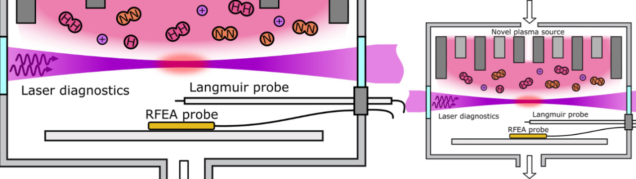
One crucial area of advancement is the development of new plasma sources for atomic-scale processing, including atomic layer deposition and etching. In this project, advanced experiments on a novel plasma source to validate plasma models will be conducted that describe the behavior of the plasma source, a step essential for advancing control and enhancing capabilities in semiconductor manufacturing.