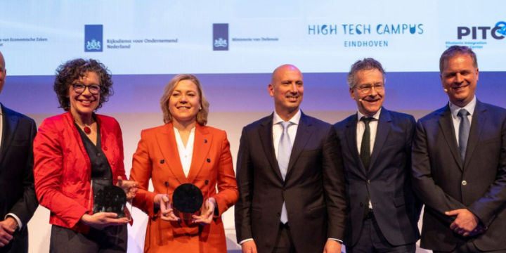
NWO awards a research project funding within the KIC call 'Demand-driven Partnerships for Consortia'. The research consortium consisting of TU Delft, ARCNL and ASML can start with innovative research that they have jointly determined: using a new technique to make the smallest details of semiconductor components visible. NWO finances the research with almost 2 million euros, the affiliated company contributes with more than 2.3 million euros in co-financing.
Smaller and more powerful
Semiconductor devices are ubiquitous in modern society and essential for technological solutions to the many challenges facing society today. Fast, accurate and precise imaging during semiconductor device fabrication is essential to make smaller and therefore more powerful devices. This also makes it possible to increase the production yield and thereby reduce costs and energy consumption.
Electrons replace light
In this project, the knowledge institutes Delft University of Technology and ARCNL are working together with high-tech company ASML to achieve improved imaging of even smaller semiconductor components. By using electrons instead of light, the highest possible resolution can be achieved for imaging the semiconductor components. Electron imaging technology still has a number of shortcomings that limit its applicability and reliability for routine use. In this research project, the consortium partners want to remedy these shortcomings.


